How it all started About PCB Design


The word PCB identifies polychlorinated biphenyl, plus its a family regarding stable industrial compounds. Common uses intended for PCBs are lubes, heat-transfer fluids, plasticizers, and solder pastes. These chemicals happen to be banned in the United States due to the fact the 1970s because of the toxic effects within the environment. Especially damaging to invertebrates and seafood, PCBs remain throughout the food chain intended for years.
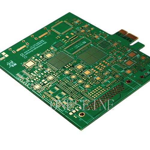
A PCB can be made from several different elements. In a typical production process, a PCB is comprised regarding a layer associated with copper, a conductive layer of indium, and a part of silver. During the fabrication process, the particular board is laminated, and then typically the soldering process requires place. The final step is a good inspection to make certain typically the PCBA works as that should. A thorough check will guarantee that the boards are free regarding any visible disorders and they are of typically the highest quality.
Branded circuit boards are produced by applying the conductive metal in order to a nonconductive area. These materials are then laminated jointly to form a new PCB. The substrate material is usually fiberglass, composite epoxy, or laminate. The conductor material about a PCB is typically copper. Copper can also be coated with tin-lead to prevent oxidation. The outer edges associated with PCBs are likewise coated with tin-leath to increase their conductivity.
Military products uses PCB's in many of applications. The equipment is regularly exposed to shock, vibration, and weighty impact. Additionally , current weapons are progressively incorporating sophisticated advanced technology. Because of this, this specific equipment requires electric powered and mechanical overall performance. The most trustworthy PCBs will withstand thousands of weight of force. When your PCB design and style is too complex or too expensive, you may desire to consider outsourced workers your PCB building.
When making some sort of PCB, it is vital to follow along with typically the JEDEC guidelines. The particular JEDEC guidelines, with regard to example, are the first step toward a PCB. They define the particular components' sizes, form, and wiring patterns. Using a PCB in a manufacturing task can be costly and time-consuming, so it is vital to realize how the device will certainly operate. When the component is not operating properly, it may lead to a crash.
Routing is the particular technique of laying copper traces between systems. Logic gates are connected through the single wire and can be connected to each other employing a conductive route. To route an association, use the online routing method throughout the PCB artist. Using the active routing command will assist you to create a more effective circuit style. Once you have a schematic, an individual can choose which usually connections need in order to be routed.
Typically the next step in PCB design is PCB layout. By simply analyzing the signal layout, you can easily create a PCB that meets the precise requirements of your own product. You have to also take directly into consideration the physical size of your own PCB. You will need to consider the space of the components on your board, so it is important to choose the best sort of material. After that, you can begin creating the circuit. You can then proceed the components about and rearrange typically the layers, based upon the electrical plus mechanical needs regarding your PCB.
The critical first step to designing PCBs will be PCB layout. Next, you can design and style a PCB structured on the schematic and select typically the appropriate materials regarding the PCB. Having an ECAD software, you can make a PCB for a variety of applications. Then, you can even generate manufacturing sketches from your PCB. You may make changes to the layout by simply altering the purchase of the elements. When the schematic is definitely complete, your circuit board is ready for manufacture.
The PCB layout needs to be improved based on the schematic and the circuit. pcb full form should minimize the number associated with wires and lessen the amount of connections. Maximum PCB layout can minimize the range of PCB alterations. You can steer clear of this problem by organizing the traces effectively. The PCB is the core regarding your electronic unit. It contains all the components that make up the circuit. Its design is the many important part of your entire product, it is therefore essential that it is designed correctly.
In addition in order to the physical results, PCBs are toxic to developing fetuses. It is achievable to pass them to a youngster through breast dairy, along with the child can certainly be afflicted with these types of contaminants. The benefits of nursing outweigh the potential risks associated with PCBs, nevertheless the effects can be extreme. pcb creation regarding young children may be greatly reduced by reducing their exposure to the chemicals. But, it is probable to reduce your risks of PCBs simply by limiting contact with PCBs while breastfeeding.