The biggest launch of the century About PCB Design


The word PCB describes polychlorinated biphenyl, in fact it is a family associated with stable industrial substances. Common uses regarding PCBs are moisturizers, heat-transfer fluids, plasticizers, and solder pastes. These chemicals are usually banned in the usa due to the fact the 1970s due to their toxic effects for the environment. Especially damaging to invertebrates and fish, PCBs remain within the meals chain intended for years.
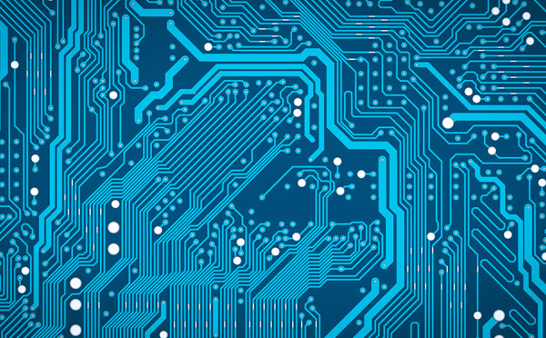
A PCB can be manufactured from several different supplies. Within a typical manufacturing process, a PCB is comprised of a layer associated with copper, a conductive layer of indium, and a part of silver. Throughout the fabrication process, the board is laminated, and then typically the soldering process can take place. The final step is a good inspection to make certain the particular PCBA works as it should. A complete check will make sure that the boards are free regarding any visible disorders and therefore are of the particular highest quality.
Branded circuit boards are made by applying a new conductive metal to be able to a nonconductive surface area. These materials are then laminated jointly to form a new PCB. The substrate material is typically fiberglass, composite epoxy, or laminate. Typically the conductor material upon a PCB is usually copper. Copper can also be coated with tin-lead to prevent oxidation. The exterior edges associated with PCBs are furthermore coated with tin-leath to increase their very own conductivity.
Military products uses PCB's in a wide range of applications. The gear is regularly put through impact, vibration, and large impact. In addition , modern day weapons are significantly incorporating sophisticated computerized technology. Therefore, this specific equipment requires electric and mechanical overall performance. The most trustworthy PCBs will tolerate thousands of lbs of force. If your PCB design and style is too intricate or too high-priced, you may desire to consider freelancing your PCB design.
When making a PCB, it is usually vital to adhere to the particular JEDEC guidelines. Tylon , with regard to example, are typically the foundation of a PCB. They define typically the components' sizes, shape, and wiring designs. Utilizing a PCB in a manufacturing job can be pricey and time-consuming, so it's vital to understand the way the device will operate. When a component is not really working properly, it may lead to a malfunction.
Routing is the particular technique of laying copper mineral traces between nodes. Logic gates are connected through a new single wire in addition to can be connected to the other person employing a conductive course. To route an association, use the interactive routing method throughout the PCB custom made. Using the fun routing command will help you to create an extra effective circuit design and style. Once you have a schematic, you can choose which usually connections need to be able to be routed.
The particular next step found in PCB design is definitely PCB layout. By analyzing the signal layout, you can create a PCB that meets the actual requirements of the product. You need to also take directly into consideration the bodily size of your PCB. You need to look at the area of the pieces on your plank, so it's important to choose the best kind of material. Next, you can start creating some sort of circuit. After that you can maneuver the components close to and rearrange the layers, based on the electrical and even mechanical needs associated with your PCB.
The critical first step to designing PCBs is usually PCB layout. Then, you can design a PCB structured on the schematic and select the appropriate materials regarding the PCB. Utilising an ECAD software, you can make a PCB for a variety of applications. Then, you may also generate manufacturing drawings from your PCB. You can create changes to be able to the layout simply by altering the purchase of the parts. After the schematic is usually complete, your circuit board is ready intended for manufacture.
The PCB layout needs to be optimized based on typically the schematic and the circuit. It will decrease the number associated with wires and lessen the amount of connections. Optimum PCB layout will certainly minimize the number of PCB changes. pcb full form can stay away from this issue by arranging the traces effectively. The PCB will be the core involving your electronic system. It has all the particular components that comprise typically the circuit. Its layout is the many important section of your current entire product, therefore it is essential that this is designed correctly.
In addition in order to the physical effects, PCBs are toxic to developing fetuses. It is probable to pass them to a kid through breast dairy, and the child can easily be troubled by these kinds of contaminants. The advantages of breastfeeding outweigh the potential risks involving PCBs, however the effects can be extreme. The health of young children could be greatly reduced by reducing their exposure to the harmful chemicals. Nevertheless, it is achievable to slow up the risks of PCBs by limiting exposure to PCBs while breastfeeding.